TYO:6920
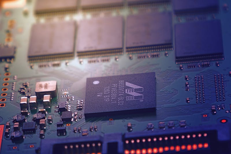
Every cutting-edge chip powering your smartphone, AI server, or autonomous vehicle passed through a single company’s inspection system before it was made. Lasertec Corporation, a Yokohama-based firm with just over 1,100 employees, holds a monopoly on the equipment that ensures EUV photomasks—the blueprints of modern semiconductors—are free of defects. Without Lasertec, the entire advanced chipmaking ecosystem would grind to a halt.
What Is EUV Lithography—and Why Does It Matter?
Extreme ultraviolet (EUV) lithography is the most advanced semiconductor manufacturing technique in use today. It uses light with a wavelength of just 13.5 nanometers—roughly 14 times shorter than the deep ultraviolet (DUV) light used in previous-generation lithography—to etch incredibly fine circuit patterns onto silicon wafers.
EUV is what makes chips at the 7nm, 5nm, 3nm, and now 2nm process nodes possible. TSMC, Samsung Foundry, and Intel all rely on EUV lithography for their most advanced products, from Apple’s A-series and M-series processors to NVIDIA’s AI accelerators and Qualcomm’s Snapdragon chips.
But EUV lithography introduces an enormous challenge: the photomask. A photomask (or reticle) is essentially the master template from which chip patterns are projected onto wafers. At EUV wavelengths, even a nanometer-scale defect on the mask can ruin an entire wafer of chips, each worth tens of thousands of dollars. The mask itself can cost $300,000 to $500,000 to produce. Ensuring it is flawless is not optional—it is existential for the economics of chipmaking.
Lasertec: The Only Company That Can Inspect EUV Masks
This is where Lasertec comes in. The company is the sole supplier of actinic EUV mask inspection systems—equipment that inspects photomasks using the same EUV wavelength (13.5nm) that will be used in production. This “actinic” approach is critical because defects that are invisible under other wavelengths can be catastrophic under EUV light.
Lasertec’s flagship product lines include:
- ACTIS A150 Series — Actinic EUV mask blank inspection system for sub-5nm processes. This system has achieved 100% global market share in its category.
- ACTIS A300 Series — Next-generation actinic EUV patterned mask inspection system, designed for 3nm and beyond, including compatibility with ASML‘s upcoming high-NA EUV lithography tools.
No other company in the world offers a commercially viable alternative for actinic EUV mask inspection. KLA Corporation, Lasertec’s closest competitor in the broader mask inspection space, does not have an actinic EUV inspection tool. This gives Lasertec an effective monopoly in one of the most critical chokepoints of the global semiconductor supply chain.
Company Overview
Founded in 1960 and headquartered in Yokohama, Japan, Lasertec Corporation (TSE: 6920) has spent over six decades developing specialized inspection and measurement instruments. The company was added to the prestigious Nikkei 225 index in 2023, a testament to its growing significance in Japan’s industrial landscape.
| Item | Detail |
|---|---|
| Founded | 1960 |
| Headquarters | Yokohama, Kanagawa, Japan |
| CEO | Osamu Okabayashi |
| Employees | ~1,163 |
| Stock Exchange | Tokyo Stock Exchange (TSE: 6920) |
| Market Capitalization | ~¥3.0 trillion (~$20B USD) |
| Nikkei 225 Inclusion | 2023 |
| Overseas Sales Ratio | >80% |
| Key Markets | Taiwan, South Korea, United States |
Sources: Lasertec Corporation IR page (lasertec.co.jp/en/ir/individuals/), Yahoo Finance (6920.T), Wikipedia — Lasertec Corporation, Statista — Lasertec net sales by region 2024
Despite having barely over 1,000 employees, Lasertec generates revenue per employee that dwarfs most semiconductor equipment companies. Taiwan—home to TSMC, the world’s largest contract chipmaker—is Lasertec’s single largest market, accounting for over ¥69 billion in net sales in FY2024. South Korea (Samsung) and the United States (Intel) follow as major customers.
Financial Performance: Explosive Growth
Lasertec’s financial trajectory over the past several years has been nothing short of extraordinary. As EUV adoption accelerated across the semiconductor industry, demand for Lasertec’s inspection systems surged in lockstep.
| Fiscal Year (ended June) | Net Sales (¥B) | YoY Growth | Operating Income (¥B) | Op. Margin | Net Income (¥B) |
|---|---|---|---|---|---|
| FY2022 | ~107.0 | — | ~31.2 | ~29% | — |
| FY2023 | ~152.8 | +42.8% | ~62.3 | ~40.8% | ~46.2 |
| FY2024 | 213.5 | +39.7% | 81.4 | 38.1% | 59.1 |
| FY2025 | 251.5 | +17.8% | 122.8 | 48.8% | 84.7 |
Sources: Lasertec Corporation consolidated financial results (FY2024 & FY2025 earnings releases), Investing.com (TYO:6920 financials), Statista — Lasertec operating income 2023, companiesmarketcap.com/lasertec/revenue/
Key takeaways from the numbers:
- Revenue more than doubled in three years, from ~¥107 billion in FY2022 to ¥251.5 billion in FY2025.
- Operating margins expanded dramatically, reaching 48.8% in FY2025—a level that rivals the most profitable software companies.
- Net profit margin hit 33.7% in FY2025, up from 27.7% in FY2024, reflecting the high operating leverage of a monopoly supplier.
- R&D investment is accelerating, with quarterly R&D expenses growing over 40% year-over-year as the company prepares for high-NA EUV.
Lasertec’s stock price reflects this performance. Between 2019 and 2024, shares surged approximately 1,800%, making it the most traded stock on the Tokyo Stock Exchange at its peak. The company’s market capitalization now hovers around ¥3 trillion (~$20 billion USD).
Why Lasertec Matters for the Global Semiconductor Supply Chain
The semiconductor industry is defined by its chokepoints—single companies or technologies without which the entire chain cannot function. ASML holds a monopoly on EUV lithography machines. TSMC dominates advanced contract manufacturing. And Lasertec holds a monopoly on the equipment needed to ensure EUV photomasks are defect-free.
Consider the implications:
- TSMC cannot manufacture 3nm or 2nm chips without verified EUV masks. Lasertec’s tools are installed at TSMC’s fabs in Taiwan.
- Samsung Foundry depends on the same inspection equipment for its Gate-All-Around (GAA) process nodes.
- Intel, in its ambitious IDM 2.0 strategy and push to regain process leadership, requires Lasertec systems for its Intel 18A and future nodes.
- ASML’s high-NA EUV (0.55 NA) systems, which began shipping in 2024, demand even more precise mask inspection—exactly what Lasertec’s ACTIS A300 series is designed to provide.
If Lasertec were unable to deliver its inspection systems, the ramp of every next-generation chip—from AI processors to mobile SoCs—would be delayed. There is no workaround. There is no alternative supplier.
The High-NA EUV Opportunity
The next frontier in EUV lithography is high-NA (numerical aperture) EUV, which uses a larger lens to print even finer features. ASML’s first high-NA EUV system, the TWINSCAN EXE:5000, has been delivered to Intel and is expected to be adopted by TSMC and Samsung in the coming years for sub-2nm nodes.
High-NA EUV creates new challenges for mask quality. The tighter tolerances mean that defects previously considered acceptable may now cause yield failures. Lasertec anticipated this transition and developed the ACTIS A300 series specifically for high-NA EUV mask inspection. The company has stated that the A300 is compatible with both current 0.33 NA and next-generation 0.55 NA EUV masks.
This positions Lasertec to capture additional revenue as the industry transitions to high-NA EUV over the next three to five years. With a backlog of ¥315.9 billion at the end of FY2025, the company has strong visibility into future demand.
Risks and Challenges
No investment thesis is without risks. For Lasertec, the key concerns include:
- Customer concentration: With the majority of revenue coming from a handful of chipmakers (TSMC, Samsung, Intel), any slowdown in their capex cycles directly impacts Lasertec.
- Order volatility: FY2025 orders fell 61.4% year-over-year to ¥105.2 billion, reflecting the lumpy nature of semiconductor equipment purchases. While the backlog remains large, new order trends bear watching.
- Competitive threats: KLA and other players are actively developing alternative EUV inspection approaches. While no commercial alternative exists today, technology shifts could erode Lasertec’s monopoly over the long term.
- Geopolitical risk: With over 80% of sales overseas—primarily in Taiwan and South Korea—Lasertec is exposed to US-China semiconductor tensions and regional instability.
- Valuation: At a market cap of ~¥3 trillion, the stock trades at a premium that prices in years of continued monopoly-level growth.
Partnership and Investment Implications
For international businesses and investors looking at the Japanese semiconductor ecosystem, Lasertec represents a uniquely compelling case study:
- For semiconductor companies: Understanding Lasertec’s product roadmap is essential for anyone planning advanced node manufacturing. Securing inspection tool allocations early could be a competitive advantage as high-NA EUV ramps.
- For component and materials suppliers: Lasertec’s growth creates opportunities in its supply chain—precision optics, EUV light sources, specialized software, and cleanroom infrastructure.
- For investors: Lasertec offers rare exposure to a monopoly position in a structurally growing market. Its inclusion in the Nikkei 225 makes it accessible to index-tracking funds, but the real story is the company’s irreplaceable role in enabling advanced semiconductors.
- For technology partners: As Lasertec invests heavily in R&D (with expenses growing 40%+ YoY), there are opportunities for collaboration in areas like AI-powered defect detection, advanced optics, and next-generation light sources.
The Bottom Line
Lasertec Corporation is one of the most strategically important—yet least understood—companies in the global technology supply chain. With 100% market share in actinic EUV mask blank inspection, revenue exceeding ¥250 billion, operating margins approaching 50%, and an essential role that no competitor can currently replicate, Lasertec is not just a Japanese success story. It is a linchpin of the AI age.
As the world races to build more powerful chips for artificial intelligence, autonomous systems, and next-generation communications, every one of those chips will depend on a mask that was inspected by a Lasertec machine. That is a position of extraordinary strategic value—and one that deserves far more global attention than it currently receives.
Explore Business Opportunities in Japan
Interested in connecting with innovative Japanese technology companies like Lasertec, or exploring partnership opportunities in Japan’s semiconductor ecosystem? Visit our Business Matching page to discover how Japonity can help bridge your business with Japan’s world-leading technology sector.
Interested in Japanese business opportunities?
Whether you're looking for technology partners, engineering talent, or market insights — we can help connect you with the right Japanese organizations.
Get in Touch →