
TYO:6965
When physicists at CERN announced the discovery of the Higgs boson in 2012, completing the Standard Model of particle physics, the detection relied on photomultiplier tubes manufactured by a mid-sized Japanese company most people have never encountered. Hamamatsu Photonics, founded in 1953 in the city that gave it its name, holds over 90% of the global market for photomultiplier tubes and has quietly become the world’s most important supplier of light-detection technology — enabling breakthroughs in particle physics, medical imaging, semiconductor manufacturing, and autonomous driving.
Origins: A Physicist’s Company From the Start
The story of Hamamatsu Photonics begins not with a business plan but with a scientific obsession. The company was founded in 1953 by Heigo Horino in Hamamatsu city, Shizuoka Prefecture, as Hamamatsu Television Co., Ltd. Horino had been a student of Kenjiro Takayanagi, the Japanese engineer credited with demonstrating the world’s first fully electronic television in 1926. Inspired by Takayanagi’s work on cathode ray tubes and photoelectric phenomena, Horino founded his company with a mission that was as much scientific as commercial: to advance the understanding and application of light.
This academic DNA has defined Hamamatsu Photonics for over seven decades. The company’s corporate philosophy, expressed in its motto “Let’s create using photonics,” reflects a belief that the detection, measurement, and manipulation of light represent a virtually inexhaustible frontier of scientific and industrial opportunity. Unlike many technology companies that pursue diversification into adjacent markets, Hamamatsu has remained relentlessly focused on a single domain: photonics.
The Photomultiplier Tube Legacy
Hamamatsu’s flagship product, and the technology that established its global reputation, is the photomultiplier tube (PMT). A photomultiplier tube is a vacuum tube that detects individual photons of light and amplifies the resulting electrical signal by a factor of up to one hundred million. This extraordinary sensitivity makes PMTs essential for scientific experiments and medical instruments that need to detect vanishingly small quantities of light.
Hamamatsu began manufacturing photomultiplier tubes in the 1950s and gradually refined the technology over the following decades. Today, the company holds over 90% of the global PMT market, a dominance that reflects both the technical difficulty of manufacturing these devices and the relatively small number of customers who require them. The PMT market is not large in absolute terms — estimated at several hundred million dollars annually — but it is strategically critical, because the experiments and instruments that depend on PMTs often have no alternative detection technology available.
Enabling Nobel Prize-Winning Physics
Hamamatsu’s most celebrated contributions have been in fundamental physics research. The company’s photomultiplier tubes have been used in some of the most important particle physics experiments of the past fifty years, including several that led directly to Nobel Prize awards.
Super-Kamiokande: The Super-Kamiokande neutrino observatory, located 1,000 meters underground in Gifu Prefecture, Japan, uses approximately 11,000 of Hamamatsu’s 20-inch photomultiplier tubes — the largest PMTs ever mass-produced — to detect the faint flashes of Cherenkov radiation produced when neutrinos interact with the observatory’s 50,000-ton tank of ultra-pure water. Data from Super-Kamiokande provided the first evidence that neutrinos have mass, a discovery that earned Takaaki Kajita the 2015 Nobel Prize in Physics.
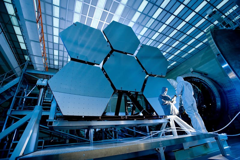
CERN and the Higgs Boson: The CERN Large Hadron Collider’s CMS and ATLAS detectors, which identified the Higgs boson in 2012, incorporate thousands of Hamamatsu photodetectors. The company supplied both traditional photomultiplier tubes and newer silicon photomultiplier (SiPM) arrays for these experiments. Peter Higgs and Francois Englert received the 2013 Nobel Prize in Physics for their theoretical prediction of the Higgs boson, confirmed by experiments that depended on Hamamatsu’s detection technology.
IceCube Neutrino Observatory: The IceCube experiment at the South Pole, which detected the first high-energy cosmic neutrinos in 2013, uses over 5,000 Hamamatsu photomultiplier tubes embedded in a cubic kilometer of Antarctic ice.
These scientific applications generate relatively modest revenue for Hamamatsu, but they serve a crucial strategic purpose: they push the boundaries of the company’s detection technology, forcing engineers to develop more sensitive, more reliable, and more specialized products that can later be adapted for commercial applications.
Financial Profile: Steady Growth in a Niche Market
Listed on the Tokyo Stock Exchange (TSE: 6965), Hamamatsu Photonics is a mid-cap company with annual revenue of approximately 200 billion yen. While this places it far below Japan’s industrial giants, the company’s profitability and growth trajectory reflect its dominant position in high-value niche markets.
| Fiscal Year | Revenue (¥B) | Operating Income (¥B) | Operating Margin |
|---|---|---|---|
| FY2020 | 155.8 | 28.2 | 18.1% |
| FY2021 | 168.5 | 34.7 | 20.6% |
| FY2022 | 204.4 | 47.5 | 23.2% |
| FY2023 | 223.5 | 49.8 | 22.3% |
| FY2024 | 201.3 | 38.9 | 19.3% |
Sources: Hamamatsu Photonics Annual Securities Reports, Tokyo Stock Exchange filings
The company’s operating margins, consistently in the high teens to low twenties, are exceptional for a hardware manufacturer and reflect Hamamatsu’s pricing power in markets where it faces limited competition. The FY2024 revenue decline was primarily driven by a slowdown in semiconductor inspection equipment demand following the post-pandemic investment cycle, a pattern seen across the semiconductor equipment supply chain.
Revenue Segmentation
Hamamatsu organizes its business into four segments, though the boundaries between them are fluid, as many products serve multiple end markets.
Electron Tube Division: Produces photomultiplier tubes, light sources, X-ray tubes, and related vacuum-based devices. This is Hamamatsu’s heritage business and the source of its scientific reputation.
Opto-semiconductor Division: Produces solid-state photodetectors, including photodiodes, avalanche photodiodes, silicon photomultipliers (SiPMs), and image sensors. This division has grown rapidly as solid-state devices increasingly complement or replace vacuum tube technologies in many applications.
Imaging and Measurement Division: Produces cameras, image processing systems, and measurement instruments for scientific, industrial, and medical applications.
Other: Includes laser devices, optical communication components, and emerging technology development.
Medical Imaging: Making the Invisible Visible
While fundamental physics experiments provide Hamamatsu with its most dramatic headlines, medical imaging represents a far larger commercial market. The company’s photodetectors are critical components in several major medical imaging modalities.
PET Scanners: Positron emission tomography (PET) scanners, used to detect cancer, assess cardiac function, and study brain activity, rely on arrays of scintillation detectors to capture the gamma rays produced when positrons annihilate with electrons inside the patient’s body. Hamamatsu supplies the photomultiplier tubes and silicon photomultipliers used in PET scanners manufactured by major medical device companies including Siemens Healthineers, GE HealthCare, and Canon Medical Systems. The company’s detectors are estimated to be present in a majority of PET scanners worldwide.
CT Scanners: Computed tomography (CT) scanners use X-ray detectors to create cross-sectional images of the body. Hamamatsu supplies photodiode arrays and scintillator-photodetector assemblies for CT systems, where detector sensitivity and speed directly affect image quality and radiation dose.
DNA Sequencing: Next-generation DNA sequencing platforms use fluorescence detection to read genetic sequences. Hamamatsu’s miniaturized photodetectors and light sources are used in sequencing instruments manufactured by Illumina and other genomics companies.
The medical imaging market provides Hamamatsu with a stable, growing revenue stream that is less cyclical than its semiconductor and industrial businesses. Global healthcare spending continues to increase, and the trend toward earlier disease detection and precision medicine drives demand for more sensitive and more capable imaging technologies.
Semiconductor Inspection: Quality Control at the Nanoscale
The semiconductor industry has become one of Hamamatsu’s most important growth markets. As chip geometries have shrunk to single-digit nanometers, the demand for ultra-precise inspection and metrology equipment has grown correspondingly. Hamamatsu supplies key optical components for semiconductor inspection systems, including photodetectors for wafer inspection tools, light sources for lithography and mask inspection, and imaging sensors for automated optical inspection systems.
The company’s products are used by leading semiconductor equipment manufacturers including ASML, KLA Corporation, and Lasertec. As the semiconductor industry invests in extreme ultraviolet (EUV) lithography and advanced packaging technologies, the requirements for optical inspection components become more demanding, playing to Hamamatsu’s strengths in high-sensitivity, high-reliability detection.
LiDAR and Autonomous Driving: The Next Frontier
Perhaps the most consequential growth opportunity for Hamamatsu lies in LiDAR (Light Detection and Ranging) systems for autonomous vehicles and advanced driver assistance systems (ADAS). LiDAR works by emitting laser pulses and measuring the time it takes for the reflected light to return, creating a three-dimensional map of the vehicle’s surroundings. The technology requires both high-power laser emitters and extremely sensitive photodetectors — both areas where Hamamatsu has deep expertise.
The company supplies laser diodes and single-photon avalanche diode (SPAD) arrays for LiDAR systems developed by automotive suppliers and autonomous driving companies. As LiDAR transitions from a niche technology used primarily in robotaxis and mapping vehicles to a standard feature in consumer automobiles, the addressable market for Hamamatsu’s components could expand by an order of magnitude.
| Application | Key Hamamatsu Products | Market Position |
|---|---|---|
| Particle Physics | PMTs, SiPMs, large-area detectors | Dominant (90%+ PMT share) |
| Medical Imaging (PET/CT) | PMTs, SiPMs, photodiode arrays | Leading supplier |
| Semiconductor Inspection | Photodetectors, light sources, sensors | Major supplier |
| LiDAR / Autonomous Driving | SPAD arrays, laser diodes | Growing presence |
| DNA Sequencing / Biotech | Mini-spectrometers, detectors | Established supplier |
| Industrial / Environmental | Flame detectors, gas analysis | Niche leader |
Sources: Hamamatsu Photonics corporate presentations, industry analysis
The Academic-Industrial Culture
What distinguishes Hamamatsu Photonics from most industrial companies is its deeply academic organizational culture. The company operates the Central Research Laboratory, which conducts fundamental research in photonics with a freedom and time horizon more typical of a university department than a corporate lab. Researchers are encouraged to pursue long-term investigations into light-matter interactions, novel detector architectures, and emerging photonic phenomena, even when commercial applications are uncertain or distant.
This culture traces directly to the founder’s vision. Heigo Horino believed that the commercial exploitation of light technology was inherently dependent on advancing the scientific understanding of light itself. He established the company’s research culture with the explicit goal of bridging the gap between academic discovery and industrial application. The company maintains close relationships with universities and research institutions worldwide, collaborating on experiments, providing custom detector solutions, and recruiting scientists who might not thrive in a purely commercial environment.
The practical result of this culture is a steady pipeline of innovations that often originate in scientific collaborations and are subsequently adapted for commercial markets. The company’s silicon photomultiplier technology, for example, was initially developed for particle physics experiments but is now finding large-volume applications in medical imaging and automotive LiDAR. This pattern of scientific innovation driving commercial products is central to Hamamatsu’s long-term strategy.
Challenges and Competitive Dynamics
Hamamatsu’s niche-focused strategy provides strong defensibility but also creates limitations. The company’s total addressable market is smaller than those of diversified electronics companies, which constrains its absolute revenue growth. The photomultiplier tube market, while dominated by Hamamatsu, is a mature technology with limited volume growth potential. Growth must come from newer product categories — silicon photomultipliers, SPAD arrays, and laser devices — where Hamamatsu faces more intense competition.
In the automotive LiDAR market, Hamamatsu competes with established semiconductor companies such as onsemi and Sony, which have significant advantages in high-volume semiconductor manufacturing. The transition from laboratory-scale production of specialized detectors to automotive-volume production of commoditized sensor arrays represents a fundamentally different operational challenge, and it remains to be seen whether Hamamatsu’s craft-oriented manufacturing culture can adapt to the cost and volume requirements of the automotive industry.
Geopolitical factors also present risks. The US-China technology competition has created export control regimes that affect the semiconductor inspection equipment market, potentially limiting Hamamatsu’s ability to sell certain products to Chinese customers. The company must navigate these restrictions while maintaining its global customer relationships.
Looking Forward: Light as Platform
Hamamatsu Photonics occupies a rare position in the global technology landscape: it is the undisputed world leader in a foundational technology — light detection — that is becoming more important with each passing year. The proliferation of autonomous vehicles, the advancement of medical imaging, the shrinking of semiconductor geometries, and the expansion of quantum computing all increase the demand for more sensitive, faster, and more specialized photonic devices.
The company’s strategy of maintaining deep technical expertise across a broad range of photonic technologies, from vacuum tubes to solid-state devices to laser systems, positions it to serve emerging applications that may not yet be foreseeable. In a world increasingly driven by the ability to detect, measure, and manipulate light, Hamamatsu’s patient, research-driven approach may prove to be the most durable competitive strategy of all.
For international businesses in medical devices, semiconductor equipment, automotive technology, or scientific instrumentation, Hamamatsu Photonics is an essential technology partner. Its product catalog, while specialized, often contains the critical enabling component that determines the performance ceiling of the final system. Understanding the company’s capabilities and technology roadmap is not merely useful — for many applications, it is indispensable.
Interested in partnering with Hamamatsu Photonics or similar Japanese companies? Contact Japonity — we connect global businesses with Japan’s most innovative companies.